Semiconductors

Faster, lighter, thinner and wearable” are words used to describe the latest trends in portable electronic devices. The same philosophy can be found in semi-conductors, printed circuits and displays to name a few. All of these improvements have been achieved in large part thanks to the use of lasers in the manufacturing processes. Excimer photolithography, laser engraving, cutting and patterning are but a few of the techniques employed to produce modern smartphones and is just one example.
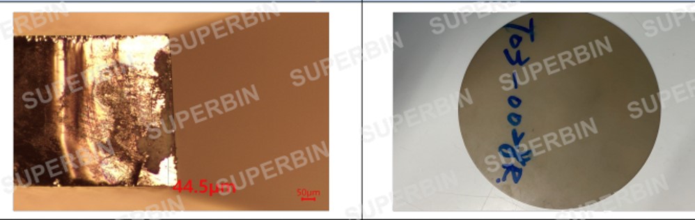
Cost, quality and throughput are major factors in achieving successful manufacturing in the semiconductor industry. With the growing adoption of new types of wafer substrates, thinner wafers and scaling to smaller dimensions and larger-size substrates, wafer dicing is evolving as a critical value-add process step that not only ensures, but also further enhances, semiconductor device yields.
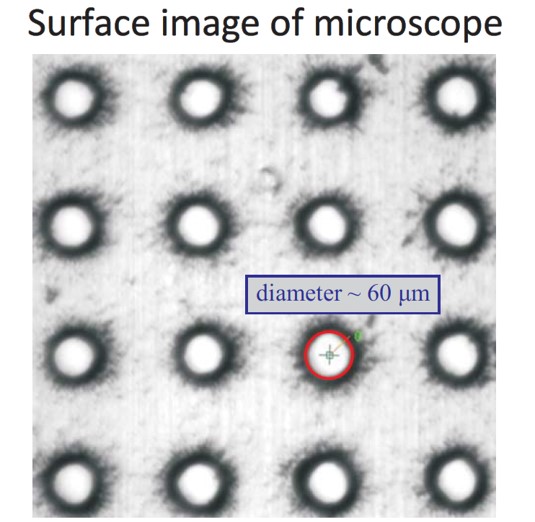
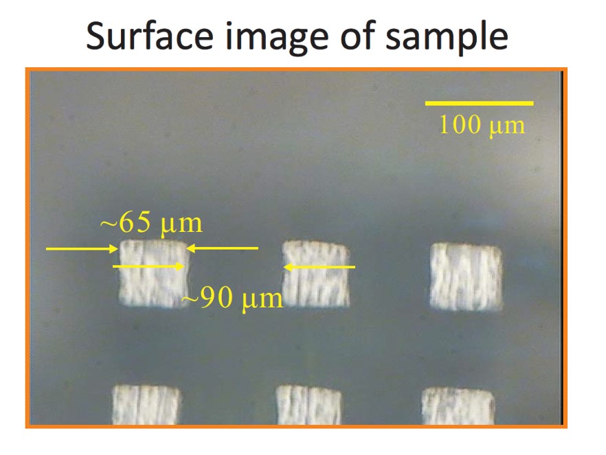
At the same time, traditional scaling of feature sizes in microelectronics is becoming increasingly cost prohibitive in order to add more functionality on devices within a smaller footprint. As a result, chip manufacturers are looking to new methods to increase device performance. Among these is the use of thermal processing to modify the surface properties of the materials in the device.